

Can an EMI shielding room be used for semiconductor device testing?
As a supplier of EMI shielding rooms, I often encounter inquiries regarding the suitability of our products for semiconductor device testing. This blog post aims to explore the feasibility and benefits of using an EMI shielding room in semiconductor device testing.
Understanding EMI Shielding Rooms
An Electromagnetic Shielding Room is a specialized enclosure designed to block electromagnetic interference (EMI) from entering or leaving the room. It is constructed using conductive materials such as steel or copper, which create a Faraday cage effect. This effect effectively shields the internal environment from external electromagnetic fields, providing a controlled and interference-free space.
Semiconductor Device Testing Requirements
Semiconductor devices, such as integrated circuits (ICs), microprocessors, and memory chips, are highly sensitive to electromagnetic interference. During the testing process, even the slightest interference can lead to inaccurate test results, false readings, and potential damage to the devices. Therefore, it is crucial to conduct semiconductor device testing in an environment that minimizes EMI.
The testing of semiconductor devices typically involves measuring electrical parameters, such as voltage, current, resistance, and capacitance, as well as evaluating the device's performance under different operating conditions. To obtain accurate and reliable test results, it is necessary to eliminate external electromagnetic noise sources and ensure a stable and controlled testing environment.
Advantages of Using an EMI Shielding Room for Semiconductor Device Testing
- Elimination of External Interference
- One of the primary advantages of using an EMI shielding room for semiconductor device testing is the elimination of external electromagnetic interference. By creating a shielded environment, the room prevents external radio frequency (RF) signals, electromagnetic pulses (EMPs), and other sources of interference from affecting the test results. This ensures that the measurements obtained are accurate and reflect the true performance of the semiconductor device.
- Enhanced Test Accuracy
- In a shielded environment, the test equipment can operate without being affected by external interference. This allows for more precise measurements and better control over the testing process. The absence of external noise sources reduces the margin of error and improves the overall accuracy of the test results.
- Protection of Sensitive Equipment
- Semiconductor testing equipment is often expensive and sensitive to electromagnetic interference. An EMI shielding room provides a protective barrier that shields the equipment from external electromagnetic fields, reducing the risk of damage and extending the lifespan of the equipment.
- Compliance with Industry Standards
- Many semiconductor manufacturers and testing laboratories are required to comply with industry standards and regulations regarding electromagnetic compatibility (EMC). Using an EMI shielding room helps ensure compliance with these standards by providing a controlled and shielded testing environment.
- Flexibility and Customization
- EMI shielding rooms can be designed and customized to meet the specific requirements of semiconductor device testing. They can be equipped with various features, such as ventilation systems, power supplies, and access ports, to facilitate the testing process and accommodate different types of test equipment.
Types of EMI Shielding Rooms for Semiconductor Device Testing
- Full-Size Shielding Rooms
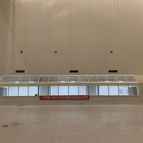
- Full-size shielding rooms are large enclosures that can accommodate multiple test stations and equipment. They are suitable for high-volume semiconductor device testing and provide a comprehensive shielded environment. These rooms can be designed to meet specific shielding requirements and can be customized with features such as modular construction, access doors, and observation windows.
- Modular Shielded Enclosures
- Modular Shielded Enclosures are smaller, pre-fabricated shielding units that can be easily assembled and disassembled. They are ideal for smaller-scale semiconductor device testing or for applications where portability and flexibility are required. Modular enclosures can be customized to fit the specific dimensions and requirements of the testing equipment and can be easily integrated into existing testing facilities.
- Partial Discharge Labs
- Partial Discharge Lab are specialized shielding rooms designed for the testing of electrical insulation materials and components. They are used to detect and measure partial discharges, which are small electrical discharges that occur within the insulation of a device. Partial discharge testing is an important part of semiconductor device testing, as it helps identify potential insulation defects and ensure the reliability and safety of the devices.
Considerations for Using an EMI Shielding Room in Semiconductor Device Testing
- Shielding Effectiveness
- When selecting an EMI shielding room for semiconductor device testing, it is important to consider the shielding effectiveness of the room. The shielding effectiveness is measured in decibels (dB) and indicates the degree to which the room can block external electromagnetic interference. The higher the shielding effectiveness, the better the protection against EMI.
- Size and Configuration
- The size and configuration of the EMI shielding room should be carefully considered based on the specific requirements of the semiconductor device testing. The room should be large enough to accommodate the test equipment and provide sufficient space for operators to move around. It should also be configured in a way that allows for easy access to the test equipment and facilitates the testing process.
- Ventilation and Cooling
- Semiconductor testing equipment generates heat during operation, and it is important to ensure proper ventilation and cooling within the EMI shielding room. Adequate ventilation helps prevent overheating of the equipment and ensures a stable and controlled testing environment. The ventilation system should be designed to minimize the introduction of external electromagnetic interference into the room.
- Power Supply and Grounding
- A reliable power supply and proper grounding are essential for the operation of the test equipment within the EMI shielding room. The power supply should be stable and free from electrical noise, and the grounding system should provide a low-impedance path for the dissipation of electromagnetic energy.
- Cost and Budget
- The cost of an EMI shielding room can vary depending on its size, configuration, shielding effectiveness, and additional features. It is important to consider the cost and budget when selecting an EMI shielding room for semiconductor device testing. However, it is also important to remember that investing in a high-quality shielding room can provide long-term benefits in terms of improved test accuracy, equipment protection, and compliance with industry standards.
Conclusion
In conclusion, an EMI shielding room can be effectively used for semiconductor device testing. It provides a controlled and interference-free environment that eliminates external electromagnetic noise sources and ensures accurate and reliable test results. The use of an EMI shielding room offers several advantages, including enhanced test accuracy, protection of sensitive equipment, compliance with industry standards, and flexibility and customization. When selecting an EMI shielding room for semiconductor device testing, it is important to consider factors such as shielding effectiveness, size and configuration, ventilation and cooling, power supply and grounding, and cost and budget.
If you are interested in learning more about our EMI shielding rooms for semiconductor device testing or would like to discuss your specific requirements, please feel free to contact us. We are a leading supplier of EMI shielding solutions and can provide you with the expertise and support you need to ensure the success of your semiconductor testing operations.

References
- "Electromagnetic Compatibility Engineering" by Henry W. Ott.
- "Semiconductor Device Physics and Design" by Simon M. Sze.
- Industry standards and regulations related to electromagnetic compatibility and semiconductor device testing.


